Category: Veronica
Veronica – RAM Board Redux
Just when you thought it was safe to call yourself Turing-complete.
Veronica seemed to be humming along nicely with her new RAM, and I was chugging away on her next set of parts. However, I started noticing strange behaviour when running test code. Things were getting a little erratic. Simple code that was clearly correct would fail to execute properly. Then the RAM test (which runs automatically on boot up) started failing sometimes. Then, she started failing to boot up at all about half the time. Something was very wrong, but with so many parts, it’s hard to know what.
When faced with a tricky problem in a complex system, a good first step is to isolate some variables. Humans don’t actually solve hard problems. We reduce them into a hundred simple ones and solve those instead. For a problem like this, form hypotheses about what might be wrong, then start testing each hypothesis to eliminate or confirm it.
The most likely culprit for my problems was the last thing I added, namely the RAM Board. The problems were new, so it made sense to aim my blamethrower on the newest part. To check that, I wrote some test code that didn’t require RAM. It just booted up and did some stuff onscreen entirely from ROM. As long as you do everything with registers and don’t try to use the stack, you can run quite a bit of 6502 code with no RAM. That code worked perfectly, so the RAM was starting to seem like the problem.
There was one other possible culprit- my shiny new backplane. Luckily, that variable was easy to eliminate, because I kept the old one intact, which was known to be reliable. I swapped in the old backplane, but the problems persisted. Further code tests confirmed that everything was fine until I tried to use RAM (either by calling subroutines, which uses the stack, or by reading and writing global variables).
So, assuming the RAM board is the problem, I started doing some very basic debugging on it. I physically inspected the board for problems, tested for shorts, double-checked continuity of all the connections against the schematic, and so forth. Everything seemed correct. However, all the evidence pointed to this board being the problem, so I pressed on. I wondered if it was a particular range of memory that was flaky. That would suggest certain address lines were bad, or one of my two RAM chips might have issues. So, I changed my boot-up RAM test code to show me which address actually fails, instead of just showing an error message:
The result was interesting, but mostly inconclusive. It was a different address each time, and the failures were all over the range of memory. So, this is not an isolated problem, which probably means my address lines and both chips are fine (or both chips are bad?). I was at an impasse.
When in doubt, start rolling back to first principles. I knew this RAM design worked, because I had it running perfectly off a breadboard. The design should be sound, but the implementation seemed to be flawed. Yet, I had verified the implementation five ways from Sunday. Well, when debugging a hard problem, remember that no assumption is sacred. When the likely suspects are exhausted, start questioning things you’re sure are correct. In this case, I needed to go back and reverify my design. Maybe I was lucky before. Maybe I hadn’t built my schematic exactly, so the etched board was wrong. Who knows.
So, out came the breadboard and the Big Box O’ Chips.

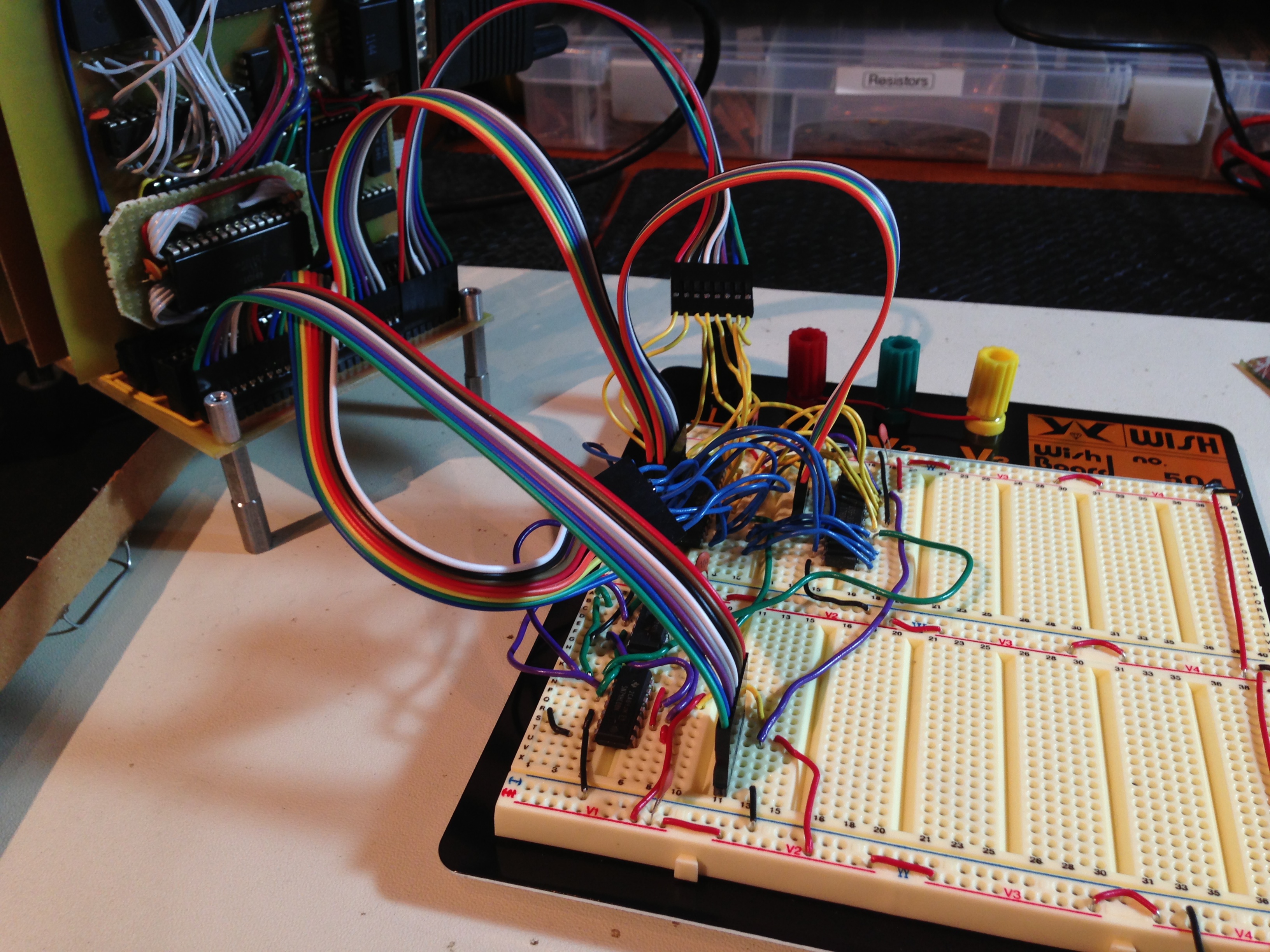
Hello sadness, my old friend. When in doubt, rebuild it on the breadboard and double-check the design.
Luckily, this sort of thing is actually quite easy for me to do, thanks to those debugging headers I stuck on the end of my bus on the backplane. That was a whim that has turned out to be one of the best decisions I’ve made on this project.
So, after all that, the RAM still didn’t work. However, some poking around with the logic probe made it immediately clear what was wrong. I had bad connections on several pins on the RAM and the decode logic. There was noise everywhere, and current draw was erratic on the power supply. Basically, I had bad connections all over the place. I was forced to admit that this loyal old breadboard is done. It’s had a hard life, having prototyped every single project you see on this site, but it’s utterly worn out. It was a discount cheapo board to begin with, and frankly it has given me grief with noise and a few flaky connections from day one.
I did some research, and tried to find the highest quality breadboard I could find. The interweb’s consensus on that seems to be Wisher’s products, so I grabbed a WishBoard from Jameco. This particular model is specifically designed for IC-heavy projects, and I’m quite impressed with the quality. You can immediately feel the difference when you insert wires. Connections are confidence inspiring, instead of the “I guess that’s in” feeling I get from the cheap breadboards.
Then I rebuilt my RAM board again on my shiny new breadboard.
My only complaint with the WishBoard is that there isn’t enough room above and below each chip to break out address and data lines (which allows you to “unwind” them for easy connection of a ribbon cable). The tradeoff is, you can get a lot more chips on a board. Still, it’s a really nice board, and a pleasure to use.
Survey says? This time, the RAM board worked perfectly. Huzzah! So, the design was sound. This was clearly an implementation problem.
At this point, I opted to cut my losses on the old board. It was an exotic double-sided board with handmade vias, none of which I had ever attempted before. The chips were all soldered down on both sides, so they were difficult to test (and could very well have been cooked with all that hand soldering). Any of a thousand things could be wrong, and it seemed easiest to just make a new board, using my older single-sided technique.
I also figured I would simplify the layout to make it easier to get right. I decided it’s time to ditch the little 32k SRAMs. I’ve been using them because they’re easy to get, and because I liked the old-school feel of multiple RAM chips lined up on the board. The 1980s computers had to do a lot of decoding and other work so that they could use large blocks of smaller chips (which were cheaper). I wanted to pay some homage to that. Well, screw homage. I just want it to work.
My loyal readers here had assured me that larger SRAMs in DIP packages are plentiful, and one very generous user even sent me some 64k chips; which the post office promptly lost. Our tax dollars at work. Well, someone please correct me if I’m wrong here, but I did a lot of looking, and I don’t think SRAMs are available in DIP packages larger than 32k that are usable for main system RAM on a reasonably fast CPU. The issue isn’t actually size, it’s speed. There’s plenty of RAM in the 150ns range, but that’s quite slow. You can get away with it at 1Mhz, but I’d like the option to go faster, and I’d like to stock one set of chips for all purposes. The video memory, for example, is hammered at 10Mhz, so even the 70ns stuff might be pushing it, by the time you get done with setup times, decoding, etc. There is some 55ns stuff out there, which I considered. There’s also lots of nice options in non-DIP packages, so I considered trying my hand at SMD soldering (which really doesn’t look that difficult).
In the end, I went with the option that involved no waiting for parts to arrive- I double-stacked some 32k chips that I had on hand. I did the same thing on my video board, and it worked swell there. They’re cheap, plentiful, and rip along at 12ns. Plenty fast for any science project that might come out of Blondihacks Labs.
I thought people might be interested in the process of making a RAM chip stack, so I snapped some photos.

I start by clamping a chip socket in the vice. This holds the chips, and also provides some heat sink for soldering. Then I carefully squish the top chip into place, making sure all the pins land in the right spots.

Chips practically beg to be stacked like this. The connections are quite solid, and work even without solder (though I solder them anyway). Note that the /CS (chip select) line is bent outwards. This is the only pin that isn’t shared, and will need a jumper down to the PCB. Now it’s just a matter of soldering each pair of pins. Be careful not to get solder too low on the pins of the lower chip, or else it won’t seat well in the socket on the PCB.
So, with one chip eliminated, my design got a lot simpler, and I could knock out a PCB in a couple of hours.

Obligatory PCB porn. I never get tired of looking at a hand-etched and hand-drilled board. I love the way these turn out.

This is easily the simplest Veronica board so far, thanks to the stacked chips. Note the upstairs jumper to the /CS line on the upper chip. Who says 3D circuits are new?
So, shiny new board all built, basic tests all passed, insert it into Veronica, fire it up, aaaaaaaaand….. FAIL. That’s right, the new board had the same problem as the original board that started all this.
What. The. Hell.
You might think I just wasted a whole lot of effort (and in some sense I did), but honestly it’s all part of the debugging process that you have to go through sometimes. By doing all this, I was very very confident that everything on that board was right. Those variables were all eliminated. That left only one culprit, no matter how improbable it seemed- the connection to the backplane.

Well, shit.
Above is a photo of my new RAM board (left), held up along side my VGA board (right). Notice anything? There’s a very slight size error in the pins of the RAM board. This error accumulates over the length of the board. At the bottom, everything looks correct. However, by the time you get to the top, the pins are out of alignment by about 40% of their width. That’s enough that they don’t line up with the backplane connector pins- sometimes. Yes, if you’re careful, there’s enough tolerance that you can get all the pins to line up. That’s why the original RAM board was flaky- it depended how the board had been jostled and how it happened to line up with the connector that day.
This is a textbook example of how, in engineering, no assumption is sacred. I’ve etched probably a dozen Veronica boards with that same edge connector template, and have never had the slightest problem with it. It has been bulletproof. So bulletproof that in all this debugging, it never even occurred to me to question it.
Well what happened here? To put it simply, I moved. Yes, I moved to a new residence recently, which means I now do my printing at a different FedEx Office branch. This new FedEx’s printers have a slightly different scale than the old ones. Of course I checked that- I’m not nuts. I check every PCB mask I make by lining up chip sockets on the paper, to make sure the printer hasn’t scaled it at all. Well, it turns out that the scaling was small enough that it didn’t show over the length of a chip socket, but does show over the length of the entire PCB. Hence the result you see above.
Ultimately, I need to build this PCB a third time. However, I want to get on with other things, and if I’m careful, this board can be lined up such that it works (as long as you don’t touch it too much). For now, that’s what I’ll do, until I have the energy to rebuild it.
If you’re not living on the edge, you’re taking up too much space, am I right?